HDI PCB / BLIND&BURIED VIA HOLE PCB / BVH PCB
|
|||||||||||||||||||||||||||||||||||||||||||||||||||||||||||||||||||||||||||||||||||||||||||||||||||||||||||||||||||||||||


|
Items |
Capability. |
|
|
Max board size |
580X700mm |
|
|
Boar Material |
FR-4,Aluminum, High Tg FR4,CEM3,etc. |
|
|
Min trace width/ space (inner layer) |
4mil/4mil(0.1mm/0.1mm) |
|
|
Min PAD (inner layer) |
5 mil(0.13mm) |
|
|
Min thickness(inner layer) |
4 mil(0.1mm) |
|
|
Inner copper thickness |
0.5~4 oz |
|
|
Outer copper thickness |
0.4~6 oz |
|
|
Finished board thickness |
0.4-3.2 mm |
|
|
Board thickness tolerance control |
±0.10 mm |
±0.10 mm |
|
±10% |
±10% |
|
|
±10% |
±10% |
|
|
Inner layer treatment |
brown oxidation |
|
|
Layer count Capability |
1-30 LAYER |
|
|
alignment between ML |
±2mil |
|
|
Drill hole diameter |
0.15mm-0.65mm |
|
|
Aspect ratio of plated hole |
10: 01 |
|
|
Hole precision |
±2 mil(±0.05mm) |
|
|
tolerance for Slot |
±3 mil(±0.75mm) |
|
|
Hole diameter tolerance(PTH) |
±3 mil(±0.075mm) |
|
|
Hole diameter tolerance(NPTH) |
±1mil(±0.025mm) |
|
|
Max Aspect Ratio for PTH |
8: 01 |
|
|
Hole wall copper thickness |
15-50um |
|
|
Alignment of outer layers |
4mil/4mil |
|
|
Min trace width/space for outer layer |
4mil/4mil |
|
|
Tolerance of Etching |
+/-10% |
|
|
Thickness of solder mask |
on trace |
|
|
Thickness of solder mask |
at trace corner |
≥0.2mil(5um) |
|
Hardness of solder mask |
On base material |
≤+1.2mil |
|
6H |
Finished thickness |
|
|
Alignment of solder mask film |
±2mil(+/-50um) |
|
|
Min width of solder mask bridge |
4mil(100um) |
|
|
Max hole with solder plug |
0.5mm |
|
|
Surface treatment |
HAL (Lead or Lead free), immersion Gold, Immersion Nickel, Electric Gold finger, plated Gold, OSP, Immersion Silver.carbon oil,etc. |
|
|
Max Nickel thickness for Gold finger |
280u"(7um) |
|
|
Max gold thickness for Gold finger |
30u"(0.75um) |
|
|
Nickel thickness in Immersion Gold |
120u"/240u"(3um/6um) |
|
|
Gold thickness in Immersion Gold |
2u"/6u"(0.05um/0.15um) |
|
|
Impedance control and its tolerance |
50±10%,75±10%,100±10% 110±10% |
|
|
Trace Anti-stripped strength |
≥61B/in(≥107g/mm) |
|
|
bow and twist |
0.75% |
|
We provide printed circuit board supplies,hdi pcb board,hdi printed circuit boards,hdi pcb prototype,hdi circuit boards,high density interconnect pcb,high density pcb,buried via pcb and buried vias pcb,RFQ today.
Persona a contactar : Molly Tu speedapcb, +86 0731 15387574935
Buen trato: comprar del vendedor
Por favor, lea nuestras condiciones de uso. También puede visitar nuestras preguntas frecuentes y ver nuestra información sobre los riesgos relacionados con la falsificación.
|
Esta página es acerca de los importadores y exportadores de HDI PCB / BLIND&BURIED VIA HOLE PCB / BVH PCB Buscar en la categoria : Varios / Descuento Buscar en la categoria : blind&buried, hole |
Reportar abuso
Saturday 20 February 2016
Cantidad : 1000 MT PE - Precio : 300/mt CIF
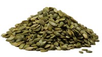
PUMPKIN SEEDS GROWN WITHOUT SHELL NEW CROP 2015 TOP GRADE AND COMPETITIVE PRICE PRODUCT DETAILS AND SPECIFICATIONS Product name Dark Green Pumpkin Seeds Year of production Crop 2016 Origin Thailand Grade A,AA grade Style Common or Organic Moisture 9%max Purity 99...
Khun Jack Partnership Ltd
- 5000 - Chaing Mai
- +66 9 68 75 20 43
Reportar abuso

Sunday 29 June 2014
La couche hybride Bio Né s'utilise avec un insert lavable ou jetable au choix. Pratique, intuitive et tendance, elle est aussi très économique car on réutilise plusieurs fois la même culotte . Ubicación : Sakiet ezzit , sfax , 3021 sfax, Persona a contactar : nada abid, +21 6 74...
Génération Eco- Innovante
- 3021 - sfax
- +21 6 74 85 93 17
- +21 6 55 35 51 38
Reportar abuso
Friday 04 March 2016
Cantidad : 150 - Precio : 550,00 €
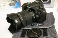
FAITS SAILLANTS DU PRODUIT 20.2MP APS-C CMOS Sensor Processeur d'image DIGIC 3.0 "Touchscreen 1,04 m-Dot Vari-Angle Full HD 1080p / 30 Vidéo & Movie Servo AF Double Pixel CMOS AF avec Live View 19-Point Toutes Croix-Type Phase-Détecter AF ISO 12800 native, étendue à la...
Electronics Design Services
- CM23 2JP - Hertfordshire
- +447405858765