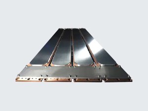
The requirements for molybdenum targets are significantly more stringent than those of conventional material industries. These requirements entail aspects including size, flatness, purity, content of impurities, density, N/O/C/S levels, grain size, and defect control. Even more rigorous or specialized requirements include surface roughness, resistance values, uniformity of grain size, composition and microstructure, foreign matter (oxide) content and size, magnetic permeability, ultra-high density, ultra-fine grains, among others.
Molybdenum sputtering coating is a newly developed physical vapor deposition technique that utilizes an electron gun system to focus and emit electrons onto the plated material. By following the momentum exchange principle, atoms are ejected out of the target surface with high kinetic energy and settle onto the substrate to form a film. The material used for the plating process is called sputtering target, which can be made from different materials such as metals, alloys, and ceramic compounds.
Types of Molybdenum Target
Planar Molybdenum Target
Purity: 99.95%
Density: ≥ 10.2 g/cm3
Size range: Customization available as required
Appearance: Microscopic examination shows the surface with uniform metallic luster, without oxidation/hydrogenation discoloration, scratches, deformation, burrs, etc.
Application: It is used to make heating parts and heat insulation parts for vacuum heat treating furnace, and to produce digesters, heaters, coolers, various utensils and devices in chemical industry. It is also extensively applied in aerospace industry, medical instruments and other fields. The sputtering target is used for magnetron sputtering coating, which is a newly developed physical vapor deposition (PVD) method.
Planar Molybdenum Target
Rotatory Molybdenum Target
Rotatory target is a kind of sputtering target. The target is made into a cylindrical shape, which is equipped with a stationary magnet inside to achieve rotatory coating at a slow speed.
We can provide molybdenum sputtering targets of the following sizes as required: length ≤ 165 mm X1000 mm, purity ≥ 99.95%.
Application: Solar cell, architectural glass, automobile glass, semiconductor, flat panel TV, etc.
Rotatory Molybdenum Target
Wide Molybdenum Target
High-purity wide molybdenum target is one of the key raw materials in the production of AMOLED panel. Our products include ultra-wide, high-purity and high-density planar molybdenum sputtering targets suitable for TFT-LCD/AMOLED, which are mainly used in G2.5-G6 generation TFT-LCD/AMOLED, thereby filling the gap of wide molybdenum target (1800 mm) in China market.
Wide Molybdenum Target
Operating Principle of Molybdenum Target
Molybdenum targets are used in the production of thin films through the process of magnetron sputtering. This process involves bombarding a metallic target with high-energy ions, which eject atoms from the target surface. These ejected atoms then deposit onto a substrate to form a thin film.
The operating principle of a mammary gland molybdenum target involves setting up a vacuum environment where the target is placed in a chamber opposite a substrate. The target is typically made of molybdenum, as it is a refractory metal that has excellent thermal and chemical stability.
Once the vacuum is established, a gas such as argon is introduced to the chamber and ionized by a magnetron sputtering source. The ionized gas is accelerated toward the molybdenum target, which causes atoms to be ejected from the surface. These ejected atoms then fly toward and deposit on the substrate to form an ultra-thin film.
The thickness and properties of the thin film can be controlled by adjusting the process parameters such as power, pressure, and gas flow rate. Molybdenum targets can be used to produce thin films in a variety of applications, from semiconductors to solar cells and medical devices.
Advantages Of Sputtering Targets
01
Versatility: Sputtering targets can deposit thin films on a variety of materials, including metals, alloys, ceramics, and semiconductors.
02
High Purity: Sputtering targets can be manufactured with high purity levels and low impurities, making them ideal for electronic and semiconductor applications.
03
Precision: The sputtering process allows for precise control over the thickness and properties of the deposited thin film.
04
Efficiency: Sputtering is a fast and efficient process, making it ideal for high-volume production applications.
05
Economic: Sputtering targets have a long service life and can be recycled, making the process an economical and sustainable way to deposit thin films.
Main Applications of Sputtering Targets
Sputtering targets are utilized in a wide range of applications, including:
Semiconductor Industry: Sputtering targets play a critical role in the production of microelectronic components and integrated circuits.
Solar Cell Industry: Sputtering targets are used in the production of solar cells to deposit thin films onto the substrate.
Display Industry: Sputtering targets are used in the production of flat-panel displays and touchscreens.
Automotive Industry: Sputtering targets are used to deposit thin films on automotive glass to improve visibility and reduce glare.
Coatings Industry: Sputtering targets are used to deposit hard, decorative, and wear-resistant coatings on a variety of substrates.
Medical Device Industry: Sputtering targets are used in the production of medical devices such as stents and pacemakers.
Overall, the versatility of sputtering targets makes them integral components in numerous industrial and technological applications.
As one of industrial cooling tower manufacturers, we will do our best to meet all the needs of customers.
Ubicación : Luoyang CBD, No.288 of Kaiyuan Avenue, Luoyang, Henan, China, 471000 luoyang,
Persona a contactar : hua Long, 037967891167


