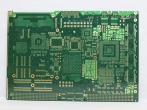
Blind & Buried VIA PCB
Cantidad : Proofing b Precio : 200-1500CNY
Custom blind and buried vias fabrication from professional and experienced pcb board supplier at low cost.
First of all, we start with traditional multi-layer boards. The structure of a standard multi-layer circuit board is a process including an inner layer line and an outer layer line, followed by drilling, and metallization in the hole to achieve the internal connection function of each layer line. However, due to the increase in line density, the way parts are packaged is constantly updated. In order to allow for a wider board area, more high-performance parts can be placed. In addition to the thinner line width, the aperture is also reduced from 1 mm in the DIP jack to 0.6 mm in SMD, and further reduced to 0.4 mm or less. However, the surface area is still occupied, so that there are buried holes and blind holes.
The Buried Holes and Blind Holes are Defined as Follows
Blind Vias: A blind via is a type of via that connects the inner trace of the PCB to the trace of the PCB surface. This hole does not penetrate the entire board.
Buried Vias: Buried vias are only connected to the type of vias between the inner layers, so they are not visible from the surface of the PCB.
Advantages of Blind Buried Hole PCB Circuit Board
Eliminate a large number of through-hole designs and increase wiring density and package density;
Diversify and complicate the design of the interconnect structure of the multi-layer board;
Significantly improved the reliability of multi-layer boards and the electrical performance of electronic products.
The Following Three Points are Distinguished for Blind Buried Plate Boards
In contrast to the through hole, the through hole refers to a hole through which each layer is drilled, and the blind hole is a non-drilled through hole.
Blind hole subdivision: blind hole, buried hole (outer layer is not visible).
Distinguish from the production process: blind holes are drilled before pressing, and through holes are drilled after pressing.
Blind buried hole technology is mainly used on relatively high-end PCBs, with high technical content and high requirements for PCB board manufacturers.
Persona a contactar : Mo Jack, +15 9 76 88 36 32
Buen trato: comprar del vendedor
Por favor, lea nuestras condiciones de uso. También puede visitar nuestras preguntas frecuentes y ver nuestra información sobre los riesgos relacionados con la falsificación.
|
Esta página es acerca de los importadores y exportadores de Blind & Buried VIA PCB Buscar en la categoria : Bienes de equipo Buscar en la categoria : blind, buried |
Monday 04 March 2013
Cantidad : 30 - Precio : $395.00
It's not just phone we're talking about... it's smart phone... it's Samsung GALAXY S III. It has the looks and a symmetry which would make you proud to hold it in your hands. You couldn't ask for more imposing façade than its 4.8 inches HD Super AMOLED high-definition display. It delivers...
Tuesday 28 April 2026
Spécifications 1. système d'amortisseur de porte 2.Material : plastique 3.Color : noir, gris, brun 4. qualité stable 5. en temps opportun vente chaude accessoires de porte d'armoiresystème tampon Matériau : plastique Couleur : noir, gris, brun Bonne qualité et le prix concurrentiel...
Chamho Industrial Co., Ltd
- 528322 - shunde
- 86 757 25523222
Thursday 03 December 2015
Cantidad : ask - Precio : ask
Health and Beauty !! pressotherapy carbon fiber material massage bed Longterm treatment is contributed to physical and mental health. Massage can relax muscle s, reduce fatigue, relieve stress, improve body blood circulation, enhance physical fitness, aerobics aging, and prolong life...
Guangzhou Yihao Electronic Technology Co., Ltd.
- eho1045
- 510385 - liwan district
- 8602081494207


