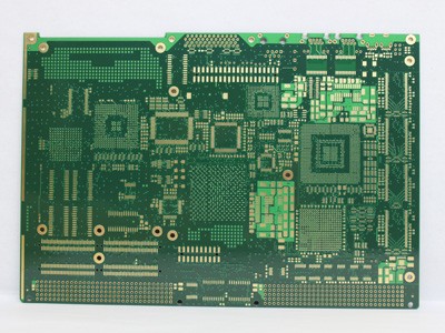


HDI PCB
Precio : 30-210 USD
HDI PCBs, one of the fastest growing technologies in PCBs, are now available at PCBSky. HDI PCBs contain blind and/or buried vias and often contain microvias of .006 or less in diameter. They have a higher circuitry density than traditional circuit boards.
There are 6 different types of HDI PCBs, through vias from surface to surface, with buried vias and through vias, two or more HDI layer with through vias, passive substrate with no electrical connection, coreless construction using layer pairs and alternate constructions of coreless constructions using layer pairs.
HDI any-layer printed circuit boards are the next technological enhancement of HDI microvia printed circuit boards: all the electrical connections between the individual layers consist of laser-drilled microvias. The main advantage of this technology is that all the layers can be freely interconnected. To produce these circuit boards, PCBSky uses laser-drilled microvias electroplated with copper.
Special Technologies Used with HDI Any-layer Printed Circuit Boards
Edge plating for shielding and ground connection
Minimum track width and spacing in mass production around 40μm
Stacked microvias (plated copper or filled with conductive paste)
Cavities, countersunk holes or depth milling
Solder resist in black, blue, green, etc.
Low-halogen material in standard and high Tg range
Low-DK Material for Mobile Devices
All recognised printed circuit board industry surfaces available
HDI PCB Technology Sheet
PCBSky HDI PCB Structures
1. 1+N+1 - PCBs contain 1 "build-up" of high-density interconnection layers.
2. i+N+i (i≥2) - PCBs contain 2 or more "build-up" of high density interconnection layers. Microvias on different layers can be staggered or stacked.
3. Copper filled stacked microvia structures are commonly seen in challenging designs.
4. Any Layer HDI - All the layers of a PCB are high density interconnection layers which allows the conductors on any layer of the PCB to be interconnected freely with copper filled stacked microvia structures ("any layer via"). This provides a reliable interconnect solution for highly complex large pin-count devices, such as CPU and GPU chips utilized on handheld and mobile devices.
PCBSky HDI PCB Capabilities: Microvias PCB
A microvia maintains a laser drilled diameter of typically 0.006" (150µm), 0.005" (125µm), or 0.004" (100µm), which are optically aligned and require a pad diameter typically 0.012" (300µm), 0.010" (250µm), or 0.008" (200µm), allowing additional routing density. Microvias can be via-in-pad, offset, staggered or stacked, non-conductive filled and copper plated over the top or solid copper filled or plated. Microvias add value when routing out of fine pitch BGAs such as 0.8 mm pitch devices and below.
Additionally, microvias add value when routing out of a 0.5 mm pitch device where staggered microvias can be used, however, routing micro-BGAs such as 0.4 mm, 0.3 mm, or 0.25 mm pitch device, requires the use of Stacked MicroVias using an inverted pyramid routing technique.
Any PCB Layer HDI
1. Multilayer copper filled stacked micro via structure
2. 3/3 mil line/space
4/8 mil laser via capture pad size
Material Options
High temperature FR4
Halogen - Free
Welcome to order HDI PCB from PCBSky at a very competitive HDI PCB price. And welcome to custom pcb fabrication from PCB MANUFACTURER CHINA.
Persona a contactar : Mo Jack, +15 9 76 88 36 32
Buen trato: comprar del vendedor
Por favor, lea nuestras condiciones de uso. También puede visitar nuestras preguntas frecuentes y ver nuestra información sobre los riesgos relacionados con la falsificación.
|
Esta página es acerca de los importadores y exportadores de HDI PCB Buscar en la categoria : Bienes de equipo Buscar en la categoria : |
Reportar abuso
Tuesday 07 July 2026
Cantidad : 108
Product Details Bed Type : Panel Layer : 2 layers Frame Material : Metal Color : Pink, Blue, Cream white, Browm… Headboard Included: Yes Under bed Storage : No Product Care : Wipe with a clean, damp cloth Painted frame · One set include - Headboard. - Footboard. - Two...
Qui Phuc Company Limited
- Luck06
- 700000 - Ho Chi Minh
- +84 9 86 58 28 62
Reportar abuso

Sunday 29 June 2014
La couche hybride Bio Né s'utilise avec un insert lavable ou jetable au choix. Pratique, intuitive et tendance, elle est aussi très économique car on réutilise plusieurs fois la même culotte . Ubicación : Sakiet ezzit , sfax , 3021 sfax, Persona a contactar : nada abid, +21 6 74...
Génération Eco- Innovante
- 3021 - sfax
- +21 6 74 85 93 17
- +21 6 55 35 51 38
Reportar abuso

Thursday 25 August 2016
Disposable Surgical Drapes We have a wide range of disposable surgical drapes for each surgical operation such as Ophthalmic, E.N.T, Gynacology, Urology, General surgery, Laparotmy, Laparoscopy, Orthopedics, Neuro, Carduvascular, Femoral, Extremity, C-section, Delivery, Spinal, T...
Egypt for medical clothes - MEDIC
- 35614 - Cairo
- +20 2 23 92 92 25